IT and software
More PCB layers bring the ground plane closer
Adding layers is not only about routing: it brings the ground plane close, and the same 50 ohms goes from a 2.85mm trace to a 0.34mm one
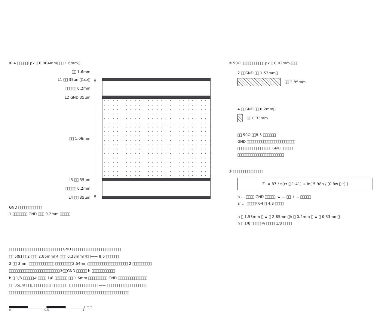
This drawing comes from one YAML file. No shape was moved by hand.
Notes in the source (in Japanese)
層を増やすのは、配線を通すためだけではない。GND を信号の真下に近づけて、線を細くするため。
同じ 50Ω が、2 層(GND まで 1.53mm)では約 2.85mm、4 層(GND まで 0.2mm)では約 0.33mm —— 8.5 倍の差。2 層で 3mm の線は、部品の足の間隔(2.54mm)より太くて引けない。
特性インピーダンスは線幅だけでは決まらない —— GND までの厚み h とセット。板厚 1.6mm は同じでも、どこに GND を置くかで線幅が変わる。
線幅は目安式から解いた(h = 1.53mm で 2.85mm は、実務で言われる 2.9〜3.1mm と一致する)。
目安式は IPC-2141A のマイクロストリップの式(0.1 < w/h < 2.0 で使える。ここでは w/h = 1.86 と 1.67 で範囲内)。εr 4.3・t 0.035mm・Z₀ 50Ω で解き直して一致を確かめた(2026-09-29)。
Source (YAML)
examples/gallery/237-基板の層構成.zumen.yaml
More in this field
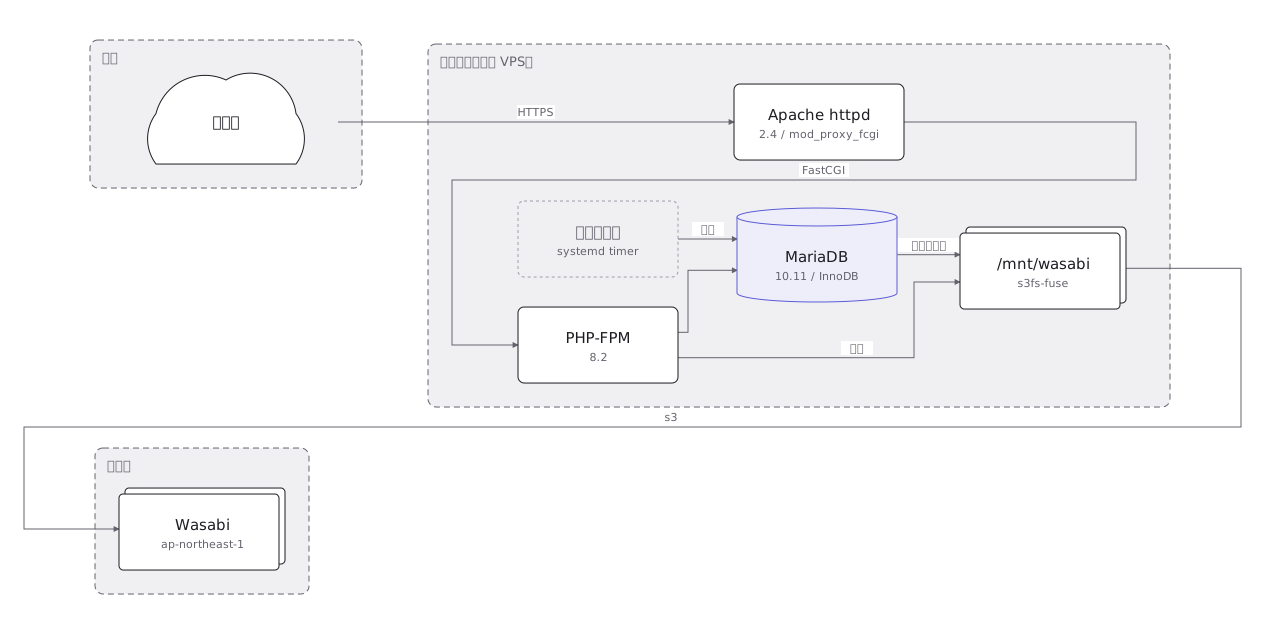 An on-premise server layout rack by rack, with the redundant power feeds and network links drawn as separate paths
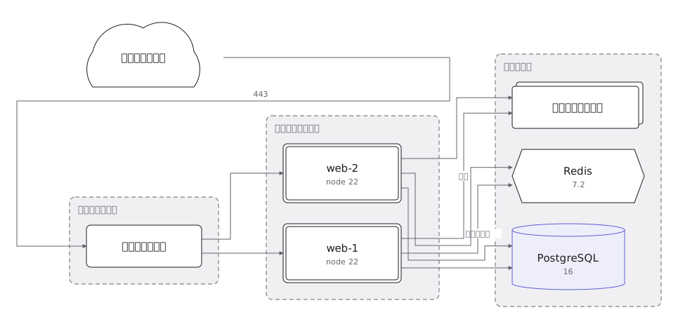 A cloud architecture showing the VPC and its subnets, and where the load balancer, application, database and object store sit
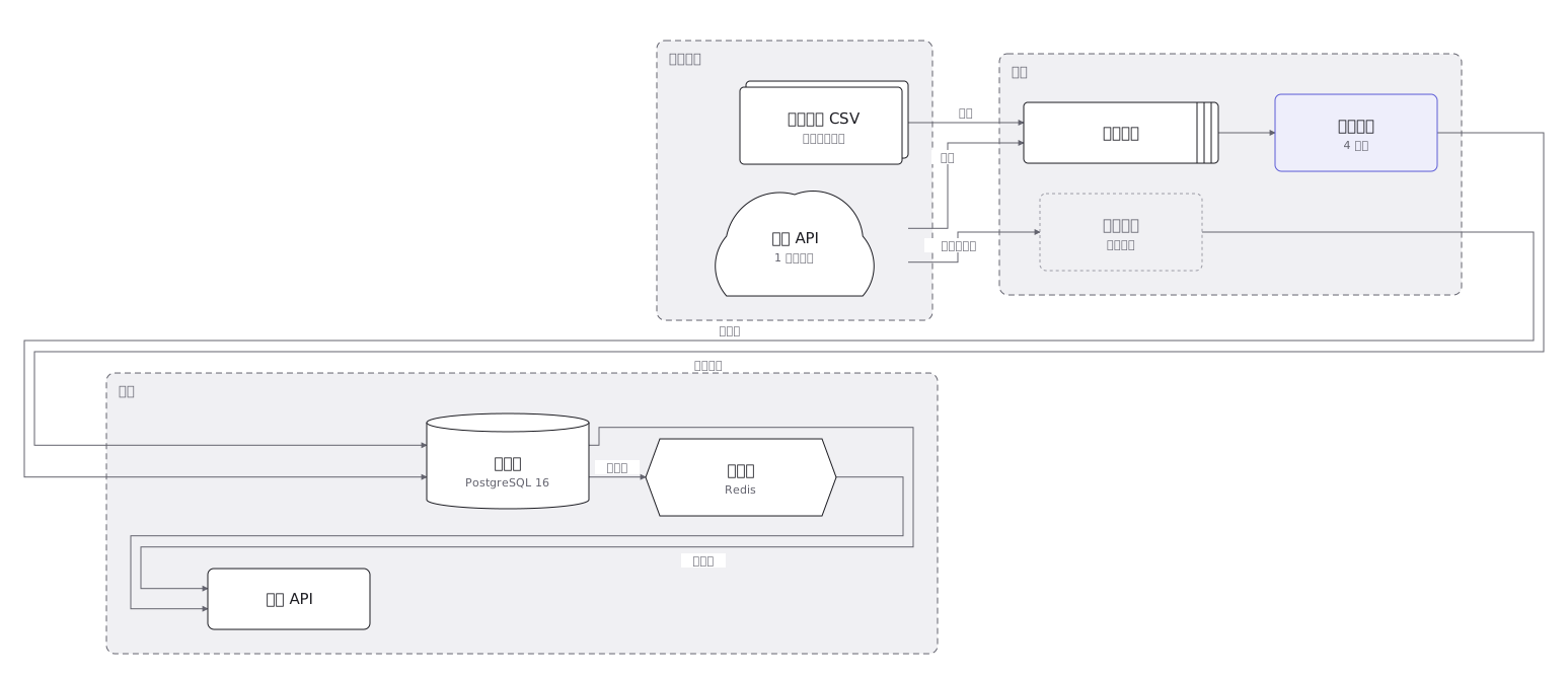 Where data goes from collection through transformation, storage and aggregation to display, and what kind of container holds it at each step
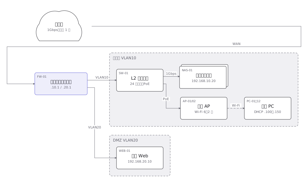 A network layout of the links and equipment between sites, with the address range carried by each segment
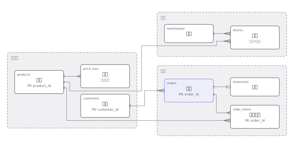 An order management ER diagram with primary and foreign keys, and the one-to-many relationships drawn as crow feet
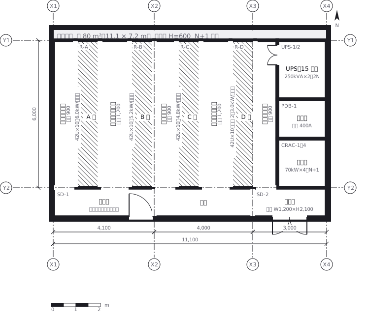 A server room where racks face each other to make hot and cold aisles, with the clearance of each aisle written in
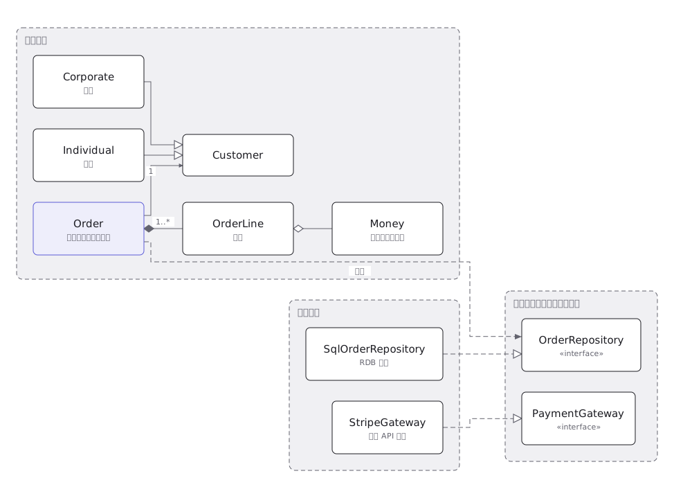 A UML class diagram where inheritance, realisation, association and aggregation are told apart by line type and end symbol
 A UML state machine with transitions, the events and guards that fire them, and the pseudostates that begin and end it