Building and civil
NAND flash hierarchy — pages and blocks
NAND flash: reads and writes go by the page, erases only by the block — every other property of an SSD follows from that mismatch
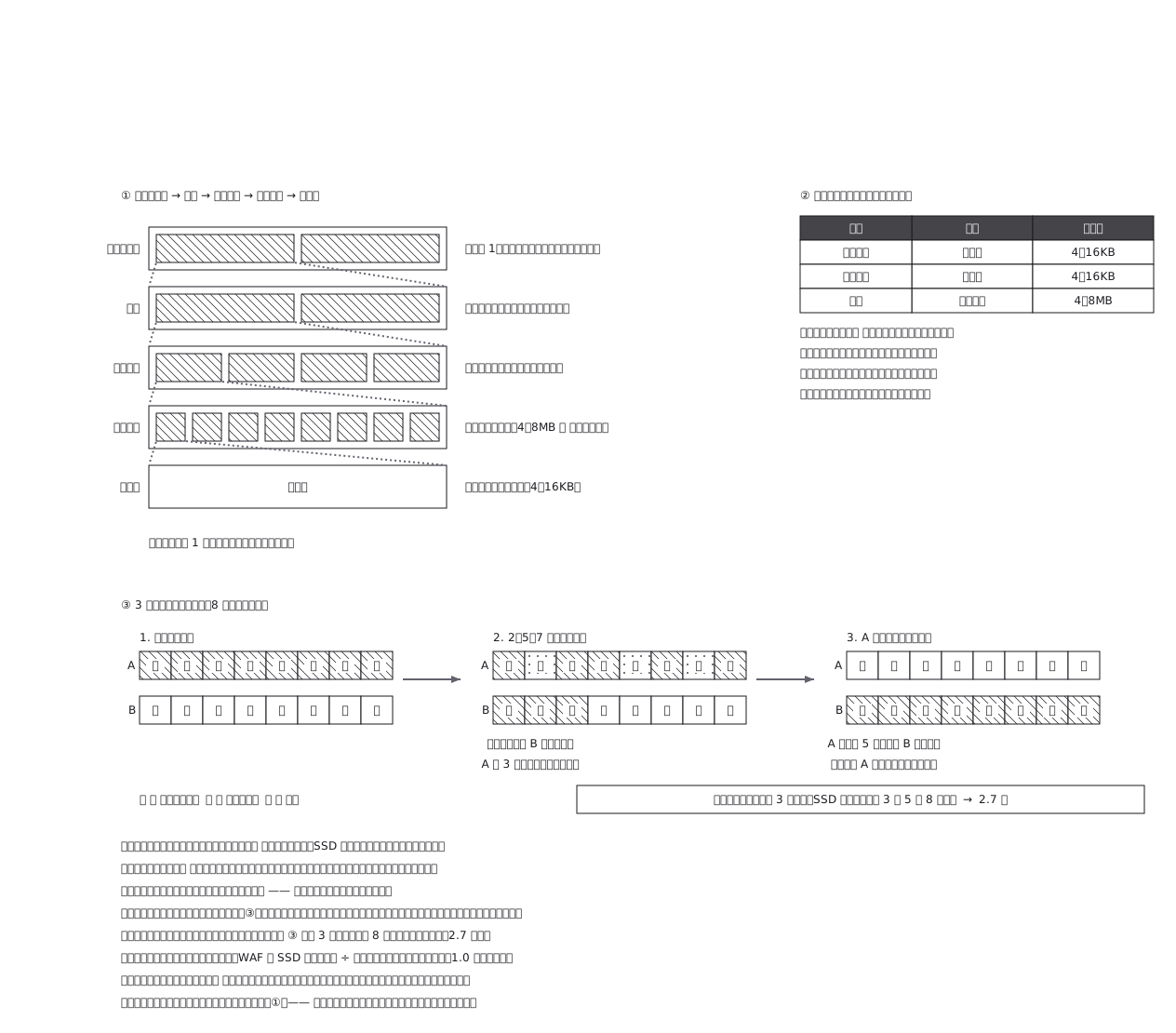
This drawing comes from one YAML file. No shape was moved by hand.
Notes in the source (in Japanese)
読み書きはページ単位、消去はブロック単位。
この食い違いから、SSD のほとんどの性質が出てくる ——上書きができない、ガベージコレクションが要る、ホストが頼んでいない書き込みが起きる(ライトアンプリフィケーション)。
1 バイト直すために、周りを読んで書き直すことになる。消去がブロック単位なので、ブロックの中の 1 ページだけを変えたくても、生きているページを別へ写してから、ブロックごと消す ——ホストが書いた量より、実際に書かれた量のほうが多くなる。
書き換えの回数に上限がある。 だから同じブロックばかり使わないように割り当てを散らす(ウェアレベリング)。SSD が「空き容量が減ると遅くなる」のも、写す先が減るため。
Source (YAML)
examples/gallery/215-NANDフラッシュの階層.zumen.yaml
More in this field
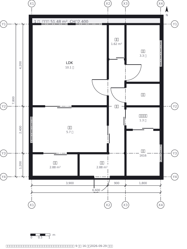 A two-bedroom apartment plan with room dimensions, which way each door swings, and where the wet rooms and storage sit
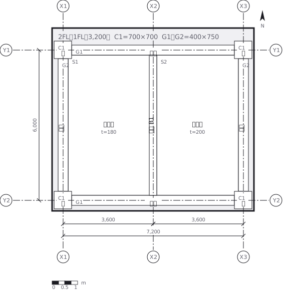 A reinforced concrete framing plan for a second floor, with the grid lines and the mark of every column, girder, beam and slab
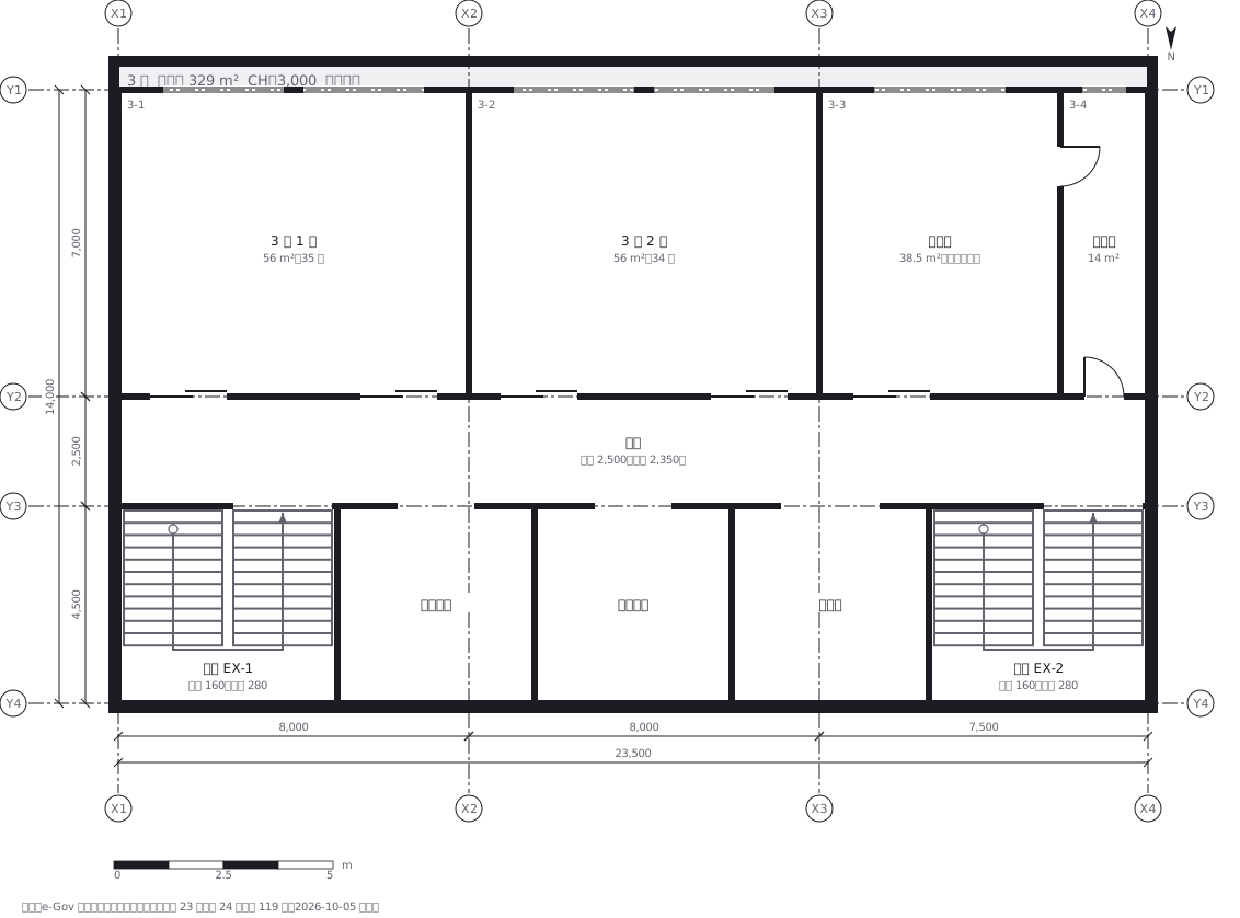 School floor plan (walls, door swings, grid lines, dimensions)
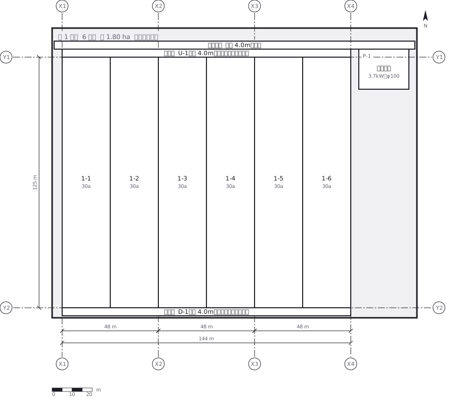 A farmland consolidation plan laying out 30-are plots, with the irrigation channels, the drainage channels and the farm roads that serve them
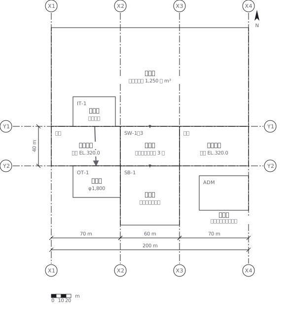 The plan of a concrete gravity dam: the body, the spillway, the intake works and the access road for maintenance
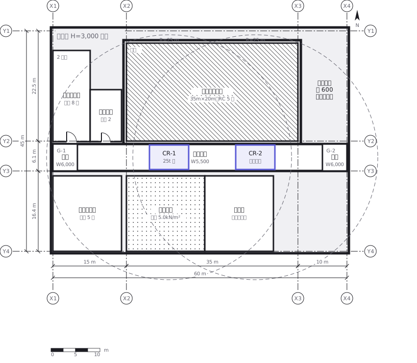 Site logistics plan with the crane radius
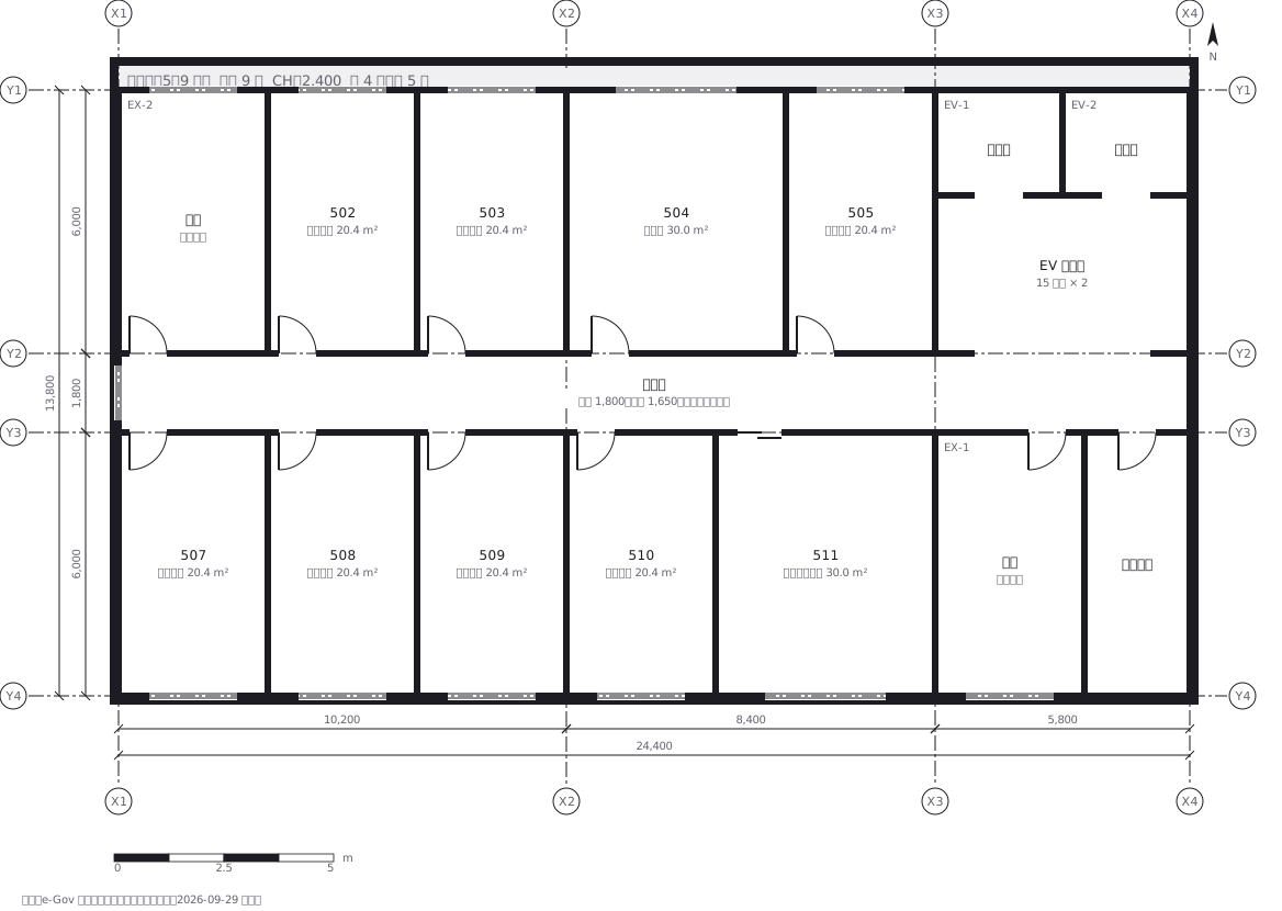 The typical floor of a business hotel with nine rooms, a central corridor, two direct stairs, and two lifts with their hall
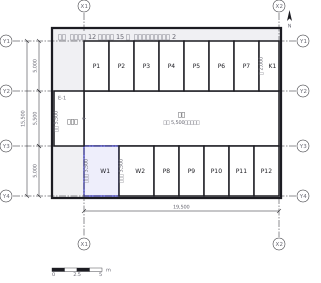 A surface car park set out for fourteen cars, with bay dimensions, aisle width and where the entrance and exit sit